Anonymous

Not logged in

  • Log in
ArmadeusWiki

APF6 SP Interfaces description

From ArmadeusWiki

Namespaces

  • Page
  • Discussion

More

  • More

Page actions

  • Read
  • View source
  • History

<< FPGA general page

Contents

  • 1 Introduction
  • 2 i.MX6 to CycloneV
  • 3 Pinouts
  • 4 Howto
  • 5 Links

Introduction

This page describe the FPGA interfaces for APF6_SP.
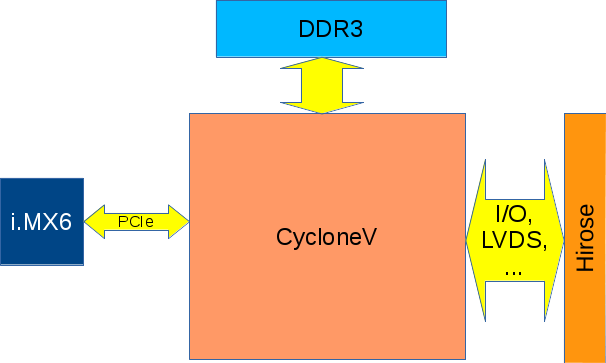
Global schematic of FPGA under APF6_SP

i.MX6 to CycloneV

  • IMX6-CycloneV interface description (PCIe)
  • DDR3-CycloneV interface description
  • APF6_SP_DMA_simple_howto

Pinouts

  • Pinout on apf6sp hirose connector
  • All pinout for PCIe, DDR3, ...

Howto

  • The full FPGA howto for the APF6_sp, with PCIe, DDR3 and I/O
  • Use JTaG USB-Blaster to access avalon bus memory on APF6_SP FPGA

Links

  • Pci debug: a tool for read/write in PCIe BAR.
Retrieved from "http://wikilegacy.armadeus.com/index.php?title=APF6_SP_Interfaces_description&oldid=15035"
Categories:
  • APF6 SP
  • FPGA
  • CycloneV
  • Quartus
  • Qsys

Navigation

Navigation

  • Main Page
  • Browse categories
  • Recent changes
  • Random page

Support/community

  • FAQ
  • Help
  • Mailing list
  • Community portal
  • Current events

Development

  • Bug tracker
  • Get latest release
  • Browse GIT repository

Wiki tools

Wiki tools

  • Special pages

Page tools

Page tools

    User page tools

      More

      • What links here
      • Related changes
      • Printable version
      • Permanent link
      • Page information
      • Page logs

      Categories

      Categories

      • APF6 SP
      • FPGA
      • CycloneV
      • Quartus
      • Qsys
      • GNU Free Documentation License 1.2
      • Powered by MediaWiki
      • This page was last edited on 5 July 2021, at 13:42.
      • Content is available under GNU Free Documentation License 1.2 unless otherwise noted.
      • Privacy policy
      • About ArmadeusWiki
      • Disclaimers