OPOS93 SP Interfaces description: Difference between revisions
No edit summary |
|||
| Line 38: | Line 38: | ||
The following chronogram depicts a burst write of the words 0xDEADBEEF, 0xCAFEBABE, 0xFEEDBEBE at 0x0102, 0x0103, 0x0104 respectively. | The following chronogram depicts a burst write of the words 0xDEADBEEF, 0xCAFEBABE, 0xFEEDBEBE at 0x0102, 0x0103, 0x0104 respectively. | ||
[[File: | [[File:flexio_armabus_burstwrite_example.png|frame|center| FlexIO Armabus 3x32b burst write]] | ||
[[Using_FPGA| << FPGA general page]] | [[Using_FPGA| << FPGA general page]] | ||
Revision as of 16:22, 9 October 2025
Introduction
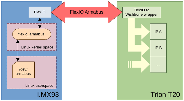
The Trion T20 FPGA is accessed by the iMX93 SoC by using a custom FlexIO bus called FlexIO Armabus.

FlexIO Armabus
The FlexIO Armabus is using FlexIO lines to design a custom 8b parallel communication bus. It consists of the following signals:
- clk: Clock of the bus. Data is shifted out on rising edge and latched on falling edge.
- add_select: Address select, next byte is an address byte.
- data_select: Data select, next byte is a data byte.
- write_enable: Write enable, 1 to write, 0 to read.
- data: Bi-directionnal 8b data.
The memory space mapped on the bus is 16 bits wide. Read/write access are done on 32b (hence 4x 8b transfer).
Read example
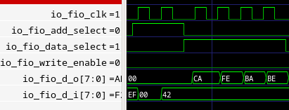
The following picture depicts a 32 bits read of the word 0xCAFEBABE at address 0x0042.

Write example
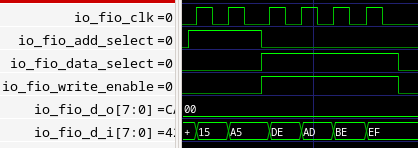
The following picture depicts a 32 bits write of the word 0xDEADBEEF at address 0x1545.

Burst mode
Address is automatically incremented after each fourth byte transferred. Please note that it is the default behavior but this can be modified in the FlexIO instance module in the FPGA design. The following chronogram depicts a burst write of the words 0xDEADBEEF, 0xCAFEBABE, 0xFEEDBEBE at 0x0102, 0x0103, 0x0104 respectively.
