OPOS93 SP Interfaces description: Difference between revisions
From ArmadeusWiki
Created page with "Category: OPOS93_SP Category: FPGA {{Under_Construction}}" |
|||
| (5 intermediate revisions by 2 users not shown) | |||
| Line 2: | Line 2: | ||
[[Category: FPGA]] | [[Category: FPGA]] | ||
== Introduction == | |||
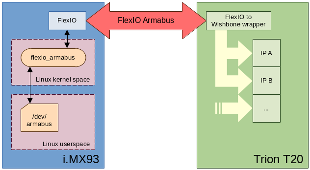
The Trion T20 FPGA is accessed by the iMX93 SoC by using a custom FlexIO bus called '''FlexIO Armabus'''. | |||
[[File:Opos93_SP_soc_fpga_diagram.png|frame|center| SoC and FPGA interface diagram for Opos93_SP]] | |||
== FlexIO Armabus == | |||
The '''FlexIO Armabus''' is using FlexIO lines to design a custom 8b parallel communication bus. It consists of the following signals: | |||
* '''clk''': Clock of the bus. Data is shifted out on rising edge and latched on falling edge. | |||
* '''add_select''': Address select, next byte is an address byte. | |||
* '''data_select''': Data select, next byte is a data byte. | |||
* '''write_enable''': Write enable, 1 to write, 0 to read. | |||
* '''data''': Bi-directionnal 8b data. | |||
The memory space mapped on the bus is 16 bits wide. | |||
Read/write access are done on 32b (hence 4x 8b transfer). | |||
=== Read example === | |||
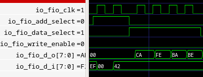
The following picture depicts a 32 bits read of the word 0xCAFEBABE at address 0x0042. | |||
[[File:flexio_armabus_read32_example.png|frame|center| FlexIO Armabus 32b read]] | |||
=== Write example === | |||
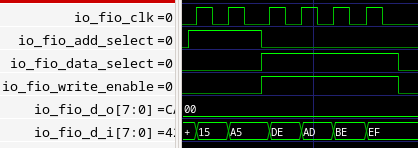
The following picture depicts a 32 bits write of the word 0xDEADBEEF at address 0x1545. | |||
[[File:flexio_armabus_write32_example.png|frame|center| FlexIO Armabus 32b write]] | |||
=== Burst mode === | |||
Address is automatically incremented after each fourth byte transferred. | |||
The following chronogram depicts a burst write of the words 0xDEADBEEF, 0xCAFEBABE, 0xFEEDBEBE at 0x0102, 0x0103, 0x0104 respectively. | |||
[[File:flexio_armabus_burstwrite_example.png|frame|center| FlexIO Armabus 3x32b burst write]] | |||
[[Using_FPGA| << FPGA general page]] | |||
Latest revision as of 16:56, 9 October 2025
Introduction
The Trion T20 FPGA is accessed by the iMX93 SoC by using a custom FlexIO bus called FlexIO Armabus.

FlexIO Armabus
The FlexIO Armabus is using FlexIO lines to design a custom 8b parallel communication bus. It consists of the following signals:
- clk: Clock of the bus. Data is shifted out on rising edge and latched on falling edge.
- add_select: Address select, next byte is an address byte.
- data_select: Data select, next byte is a data byte.
- write_enable: Write enable, 1 to write, 0 to read.
- data: Bi-directionnal 8b data.
The memory space mapped on the bus is 16 bits wide. Read/write access are done on 32b (hence 4x 8b transfer).
Read example
The following picture depicts a 32 bits read of the word 0xCAFEBABE at address 0x0042.

Write example
The following picture depicts a 32 bits write of the word 0xDEADBEEF at address 0x1545.

Burst mode
Address is automatically incremented after each fourth byte transferred. The following chronogram depicts a burst write of the words 0xDEADBEEF, 0xCAFEBABE, 0xFEEDBEBE at 0x0102, 0x0103, 0x0104 respectively.
